Thanks to graphene – the strongest and thinnest material currently known in science – semi-transparent, flexible electronics may no longer be just science fiction, say researchers from the University of Sheffield and the University of Manchester, both in England.
The scientists wrote in the academic journal Nature Materials (citation below) that new 2D “designer materials” can be made to create see-through, flexible and more efficient electronic devices.
Team leader, Nobel Laureate Sir Kostya Novoselov, and colleagues made the breakthrough by creating light-emitting diodes (LEDs) that had been engineered on an atomic level.
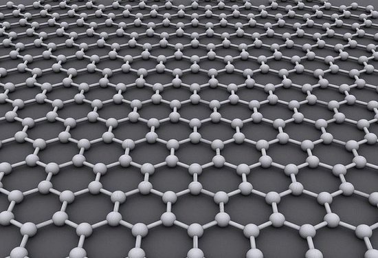 Graphene, a single layer of pure carbons arranged in a hexagonal lattice pattern, is 200 times stronger than steel. It is the thinnest and lightest material in the world. It is so thin that it is considered to be a 2-dimensional object. (Image: Wikipedia)
Their latest research demonstrates that graphene and related two-dimensional materials could be used to create light-emitting devices for the next generation of TVs, tablets and mobile phones to make them super-thin, durable, flexible and even transparent.
They built the LED device, which emits light from across its whole surface, by combining different 2D crystals. These components, which are only between 10 and 40 atoms thick, can form the basis for the first generation of semi-transparent smart devices.
Researchers at the University of Manchester first isolated and explored one-atom thick graphene in 2004. Graphene has potential for being used in a vast range or areas, the most likely being electronics.
Since 2004, other 2D materials, such as molybdenum disulphide and boron nitiride have been discovered, opening up huge areas of research and potential applications.
By building heterostructures – stacked layers of several two-dimensional materials – to create targeted functionality and introducing quantum wells to control electron movements, new potential uses for graphene based optoelectronics (combined use of electronics and light) have now been realized.
 LED Heterostructure Schematic. (Image: University of Manchester)
Freddie Withers, a Royal Academy of Engineering Research Fellow at The University of Manchester, who led the production of the devices, said:
“As our new type of LED’s only consist of a few atomic layers of 2D materials they are flexible and transparent. We envisage a new generation of optoelectronic devices to stem from this work, from simple transparent lighting and lasers and to more complex applications.”
Sir Kostya said, regarding the creation of the LED device:
“By preparing the heterostructures on elastic and transparent substrates, we show that they can provide the basis for flexible and semi-transparent electronics.”
“The range of functionalities for the demonstrated heterostructures is expected to grow further on increasing the number of available 2D crystals and improving their electronic quality.”
Professor Alexander Tartakovskii, who works at the University of Sheffield added:
“The novel LED structures are robust and show no significant change in performance over many weeks of measurements. Despite the early days in the raw materials manufacture, the quantum efficiency (photons emitted per electron injected) is already comparable to organic LEDs.”
Citation: “Light-emitting diodes by band-structure engineering in van der Waals heterostructures,” F. Withers, O. Del Pozo-Zamudio, A. Mishchenko, A. P. Rooney, A. Gholinia, K. Watanabe, T. Taniguchi, S. J. Haigh, A. K. Geim, A. I. Tartakovskii & K. S. Novoselov. Nature Materials. Published Feb 2, 2015. DOI:10.1038/nmat4205.