Researchers from Denmark and Japan have achieved a breakthrough in graphene-based nanoelectronics. They have solved one of the major challenges that baffled scientists.
The researchers wrote about their work in the prestigious journal Nature Nanotechnology (citation below).
Scientists have been trying to exploit graphene, the ‘miracle material,’ to produce nanoscale electronics for many years. If something is ‘nanoscale,’ it is super-small. A nanometer is one billionth of a meter (10-9 meter).
In theory, graphene should be great for nanoelectronics. It is the thinnest material in the world – just one atom thick. Scientists describe it as two-dimensional.
It is also an excellent conductor of electricity and holds great promise for future state-of-the-art electronics. In other words, more energy efficient and faster electronics.
Additionally, graphene consists of carbon atoms. Our planet has lots of carbon atoms.
Graphene-based nanoelectronics – one major difficulty
Theoretically, we can alter graphene to perform several different tasks within, for example, photonics, electronics, and sensors. All we have to do is cut tiny patterns in it, which fundamentally alters graphene’s quantum properties.
One seemingly ‘simple task,’ however, has turned out to be extremely difficult. That is, to induce a band gap, which is essential for making optoelectronic devices and transistors.
However, given that graphene is just one atom thick, all its atoms are important. Therefore, even super-tiny irregularities in the pattern can destroy its properties.
Prof. Peter Bøggild, from the Technical University of Denmark’s (DTU’s) Department of Physics, said:
“Graphene is a fantastic material, which I think will play a crucial role in making new nanoscale electronics. The problem is that it is extremely difficult to engineer the electrical properties.”
The Center for Nanostructured Graphene was established in 2012 at Aalborg University and DTU, both in Denmark. Its goal was to study how graphene’s electrical properties could be tailored by altering its shape at the nanoscale.
However, when patterning graphene, Aalborg and DTU scientists faced the same problem as other researchers – it did not work.
Patterning graphene alters it too much
Prof. Bøggild said:
“When you make patterns in a material like graphene, you do so in order to change its properties in a controlled way – to match your design. However, what we have seen throughout the years is that we can make the holes, but not without introducing so much disorder and contamination that it no longer behaves like graphene.”
“It is a bit similar to making a water pipe that is partly blocked because of poor manufacturing. On the outside, it might look fine, but water cannot flow freely. For electronics, that is obviously disastrous.”
Problem solved
Two Postdocs from DTU Physics, Lene Gammelgaard and Bjarke Jessen, have solved the problem. They first encapsulated the graphene inside hexagonal boron nitride, another 2-D material. Scientists frequently use hexagonal boron nitride to protect graphene’s properties.
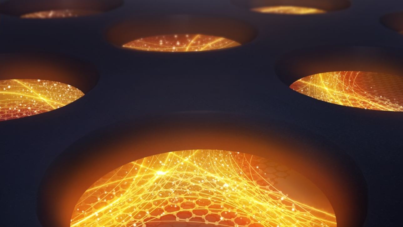
Then, they used electron beam lithography to carefully pattern the outer layer of boron nitride and the graphene below with a dense array of tiny holes. The holes, which were 12 nanometers apart, had a diameter of about 20 nanometers.
The roughness at the edges of these holes, however, was less than one nanometer. This meant that 1,000 times more electrical current could flow than had been reported in such tiny graphene structures.
Graphene-based nanoelectronics – curse lifted
Prof. Bøggild said:
“We have shown that we can control graphene’s band structure and design how it should behave. When we control the band structure, we have access to all of graphene’s properties – and we found to our surprise that some of the most subtle quantum electronic effects survive the dense patterning – that is extremely encouraging.”
“Our work suggests that we can sit in front of the computer and design components and devices – or dream up something entirely new – and then go to the laboratory and realize them in practice.”
“Many scientists had long since abandoned attempting nanolithography in graphene on this scale, and it is quite a pity since nanostructuring is a crucial tool for exploiting the most exciting features of graphene electronics and photonics. Now we have figured out how it can be done; one could say that the curse is lifted.”
“There are other challenges, but the fact that we can tailor electronic properties of graphene is a big step towards creating new electronics with extremely small dimensions.”
Citation
“Lithographic band structure engineering of graphene,” Bjarke S. Jessen, Lene Gammelgaard, Morten R. Thomsen, David M. A. Mackenzie, Joachim D. Thomsen, José M. Caridad, Emil Duegaard, Kenji Watanabe, Takashi Taniguchi, Timothy J. Booth, Thomas G. Pedersen, Antti-Pekka Jauho, and Peter Bøggild. Nature Nanotechnology (2019). 18 February 2019. DOI: https://doi.org/10.1038/s41565-019-0376-3.
