Did you recently have a PCB design that had some interference issues, and you are lost in the sea of circuits and traces? Well, just stepped into the ocean of HIGH-SPEED PCB DESIGN. Because the delivery time for each system in a PCB design is not as you calculated should not make you lose sleep. You would be walked through some of the fundamental problems that you might encounter when designing a high-speed PCB.
But before we sink our teeth into the meat, what is high-speed PCB?
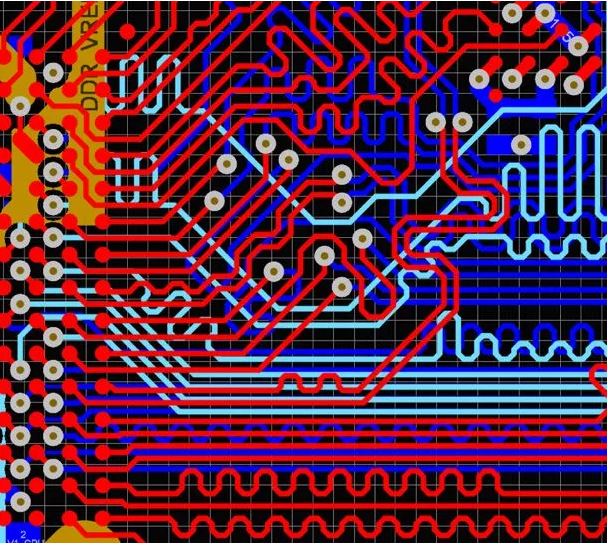
Integrasources.com says that all high-tech devices are designed with high-speed PCB due to the small size of the equipment and the need for faster data transfer. Ni.com defines PCB design as a rugged copper and non-conductive substrate-based structure to connect electrical components. High-Speed PCB is, therefore, a high-speed PCB design where the integrity of your signals starts to be affected by the physical characteristics of your circuit board.
While in the conventional PCB designs, engineers are focused on the placement of components and routing, with High-Speed PCB designs, the installation of the traces, their width, and their proximity are crucial.
Characteristics of High-Speed PCB Design
- Digital frequency is 50MHz and over.
- The size of the printed circuit board is small; therefore, the location of components becomes a problem.
- It has several sub-circuits that work independently connected
- High-speed interface
- Signal propagation time over the track is at least 1/3 of the signal rise time.
These characteristics, if present in circuit design, makes it a High-Speed PCB design.
Physical Characteristics That May Affect Signal Integrity
- Layer startup
- Packaging
- Interconnections
Some of the issues you would encounter in a high-speed PCB design include:
- Timing: This factor is imperative because the time each signal arrives at the endpoint will either make your work easier or harder. If the arrival time is wrong, probably affected by the proximity of the copper wires, then you get corrupted data.
- Integrity: Signals are either digital or analog. While the digital signal is referred to as a square wave or clock signal, and are simpler to understand, analog signals are a set of range of positive and negative values. If the appearance of these signals is not as it is supposed to when they arrive at their destination, then it means there has been interference on its journey to the endpoint.
- Noise: Every PCB emits some sound, but too much noise, mainly due to interference, affects the signal quality and reliability.
To fix these significant problems you might experience while deigning high-speed PCB, here are three solutions to noise, integrity, and Timing:
- Spacing: This solves the issue of noise. When you space the traces on your circuit, you reduce the probability of noise and other forms of signal interference.
- Impedance: impedance is a form of resistance in an electrical circuit. This resistance depends on frequency. The right impedance between the transmitter and receiver improves the quality of the signal and reduces the noise.
- Matching: The length of two coupled traces should be matched to guarantee that signals arrive at the same time.
The high-Speed PCB design is complicated as it is exciting. In a world where speed and portability lead the way, having an effective high-speed PCB design that eliminates the issues mentioned above is necessary. It requires attention to detail and following the simple principles of High-Speed PCB designs.
_______________________________________________________
Interesting related article: “What is Technology?“