

The performance of 2-dimensional material MoS2 (molybdenum disulfide) can be significantly improved by encapsulation in boron nitride, say scientists from the US, Japan, Denmark and South Korea.
Two years ago, Wang Fong-Jen, James Hone, and colleagues at Columbia University explained that Graphene’s performance could be improved dramatically by encapsulating it in boron nitride, an insulating material with a similar layered structure to the highly conducting 2-D carbon.
This study’s leader, Prof. Hone, who is director of Columbia’s NSF-funded Materials Research Science and Engineering Center, said:
“These findings provide a demonstration of how to study all 2D materials. Our combination of BN and graphene electrodes is like a ‘socket’ into which we can place many other materials and study them in an extremely clean environment to understand their true properties and potential.”
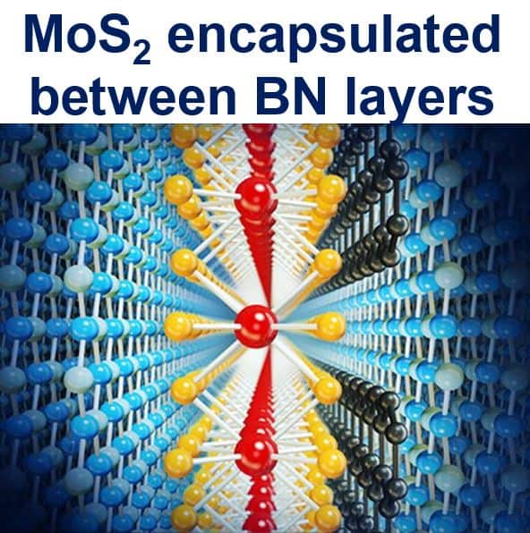
MoS2 (Molybdenum disulfide) encapsulated between layers of boron nitride. (Credit: Gwan-Hyoung Lee/Yonsei University)
“This holds great promise for a broad range of applications including high-performance electronics, detection and emission of light, and chemical/bio-sensing.”
2-D materials created by ‘peeling’ atomically thin layers from bulk crystals are super stretchable, visually transparent, and can be combined with each other and with conventional electronics in completely novel ways.
However, these two-dimensional materials, in which all the atoms are at the surface, are by their very nature extremely sensitive to their environments, which means that their performance frequently falls far short of theoretical limits, because of contamination and trapped charges surrounding insulating layers.
When Prof. Hone and colleagues encapsulated graphene with BN last year, electronic mobility improved by a factor of fifty – an important measure of electronic performance – and lower disorder that enables the study of rich new phenomena at low temperature and high magnetic fields.
MoS2 can be switched fully ‘off’
Gwan-Hyoung Lee, co-lead author on the Nature Nanotechnology paper, and assistant professor of materials science at Yonsei University, Seoul, South Korea said:
“We wanted to see what we could do with MoS2 – it’s the best-studied 2D semiconductor, and, unlike graphene, it can form a transistor that can be switched fully ‘off’, a property crucial for digital circuits.”
Previously, MoS2 devices made on common insulating substrates, such as silicon dioxide, have shown mobility that falls below theoretical predictions, fluctuates from sample to sample, and stays low upon cooling to low temperatures – all indications of disordered materials.
Scientists have not known whether the disorders occurred because of the substrate, as in the case of graphene, or from imperfections in the material itself.
In this latest study, Prof. Hone and colleagues created heterostructures, or layered stacks, of MoS2 encapsulated in BN, with tiny flakes of graphene overlapping the edge of the MoS2 to act as electrical contacts.
The researchers found that at room temperature mobility improved by a factor of around 2, approaching the intrinsic limit.
When it cooled to a low temperature, the mobility increased significantly, reaching values five to fifty times greater than those measured previously (depending on the number of atomic layers).
As a further sign of low disorder, these high-mobility samples also showed strong fluctuations in resistance with magnetic field, which had never been seen before in a 2D semiconductor.
First author Xu Cui, a PhD student at Columbia Engineering, said:
“This new device structure enables us to study quantum transport behavior in this material at low temperature for the first time.”
Further improvements possible
After analyzing the low-temperature resistance and quantum oscillations, Prof. Hone and team concluded that the main source of the disorder remained contamination at the interfaces, suggesting that further improvements were possible.
Prof. Hone said:
“This work motivates us to further improve our device assembly techniques, since we have not yet reached the intrinsic limit for this material.”
“With further progress, we hope to establish 2D semiconductors as a new family of electronic materials that rival the performance of conventional semiconductor heterostructures – but are created using scotch tape on a lab-bench instead of expensive high-vacuum systems.”
In Italy, a team of scientists sprayed spiders with a solution of water and graphene. The spiders produced incredibly strong webs, strong enough to catch a falling airplane.
Citation: “Multi-terminal transport measurements of MoS2 using a van der Waals heterostructure device platform,” Xu Cui, Gwan-Hyoung Lee, Young Duck Kim, Ghidewon Arefe, Pinshane Y. Huang, Chul-Ho Lee, Daniel A. Chenet, Xian Zhang, Lei Wang, Fan Ye, Filippo Pizzocchero, Bjarke S. Jessen, Kenji Watanabe, Takashi Taniguchi, David A. Muller, Tony Low, Philip Kim & James Hone. NATURE NANOTECHNOLOGY. Published 27 April, 2015. DOI: 10.1038/nnano.2015.70.