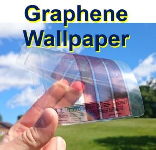

An amazing graphene wallpaper that could power your home from electricity generated from waste light or heat, even in dim conditions, is being developed by a team of scientists at the Advanced Technology Institute, University of Surrey, England. Imagine how much power-plant generation could be saved if every home in the country had this hi-tech wallpaper.
Graphene, the thinnest and strongest material we know about, can also be manipulated to create the most light-absorbent material (for its weight) on Earth. The nanometre-thin material could be used to power a host of applications from today’s ever-growing list of ‘Internet of Things’.
The Internet of Things is a a proposed development of the Internet in which everyday objects have network connectivity, allowing them to receive and send data.
 Imagine a graphene wallpaper in your home that absorbs ambient light and heat, even in dim conditions, and generates electricity. (Image: eurekalert.org)
Graphene – an incredible material
Graphene is an incredible new material consisting of a single layer of pure carbon atoms. They are all arranged in a hexagonal (six-sided) lattice pattern. Scientists say it is the strongest, lightest and thinnest material they know about. It is 207 times stronger than steel.
A team of scientists explained in the peer-reviewed journal Science Advances (citation below) how they took inspiration from nature to create super-thin graphene sheets designed to capture light more effectively.
They used a technique called nanotexturing, which involves growing graphene around a textured metallic surface – the material is covered with nano-sized structures, i.e. structures that are so thin they have just one dimension.
Grapehene might be ultra-strong, but traditionally it has not been efficient at absorbing light. To overcome this, co-author Professor Ravi Silva, Head of the Advanced Technology Institute, and colleagues used the nano-patterning to localize light into the narrow spaces between the textured surface, thus increasing the amount of light the material could absorb by approximately 90%.
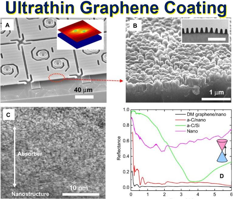 (A) TPS design with raised surface. Inset: hot scale, 20°C (blue); 800°C (red). (B) Top surface of TPS showing nanostructured ultrathin absorber. (C) High-resolution scanning transmission electron microscopy (HR-STEM) from top of nanostructures, showing the graphene planes of the optical absorber layer. (D) Reflectance for the decoupled multilayer (DM) graphene surrounding the metal nanostructures (black curve), uncoated nanostructures (pink), nanostructures coated with amorphous carbon (a-C) (red), and a-C on a plain silicon substrate. The DM graphene absorber (black curve) shows broadband antireflection. (Image: Science Advances)
Inspiration from moths’ eyes
Prof. Silva said:
“Nature has evolved simple yet powerful adaptations, from which we have taken inspiration in order to answer challenges of future technologies. Moths’ eyes have microscopic patterning that allows them to see in the dimmest conditions.”
“These work by channelling light towards the middle of the eye, with the added benefit of eliminating reflections, which would otherwise alert predators of their location. We have used the same technique to make an amazingly thin, efficient, light-absorbent material by patterning graphene in a similar fashion.”
Graphene has been described by many as the Holy Grail for future technology. It has been found to have amazing electrical conductivity capabilities, impressive mechanical strength, a wide range of electronic applications, used to make microphones 32 times more sensitive than current ones, make a web that can catch a falling airplane, improve energy storage, and used to make cheaper and more durable light bulbs.
Graphene must harvest light and heat
Prof. Silva and colleagues understood that for graphene to be fully exploited as a material for future applications, it should also harness heat and light effectively.
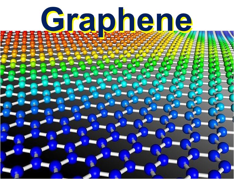 According to Graphenea: “In simple terms, graphene, is a thin layer of pure carbon; it is a single, tightly packed layer of carbon atoms that are bonded together in a hexagonal honeycomb lattice. In more complex terms, it is an allotrope of carbon in the structure of a plane of sp2 bonded atoms with a molecule bond length of 0.142 nanometres.” (Image: britishcarbon.org)
Prof. Silva explained:
“Solar cells coated with this material would be able to harvest very dim light. Installed indoors, as part of future ‘smart wallpaper’ or ‘smart windows’, this material could generate electricity from waste light or heat, powering a numerous array of smart applications.”
The research team believes that new types of sensors and energy harvesters connected through the Internet of Things would also benefit from this kind of coating.
Lead author, Dr. José Anguita, who works at the Advanced Technology Institute’s Nanoelectronics Centre, commented:
“As a result of its thinness, graphene is only able to absorb a small percentage of the light that falls on it. For this reason, it is not suitable for the kinds of optoelectronic technologies our ‘smart’ future will demand.”
“Nanotexturing graphene has the effect of channelling the light into the narrow spaces between nanostructures, thereby enhancing the amount of light absorbed by the material. It is now possible to observe strong light absorption from even nanometre-thin films.”
“Typically a graphene sheet would have 2-3% light absorption. Using this method, our ultrathin coating of nanotextured few-layer graphene absorbs 95% of incident light across a broad spectrum, from the UV to the infrared.”
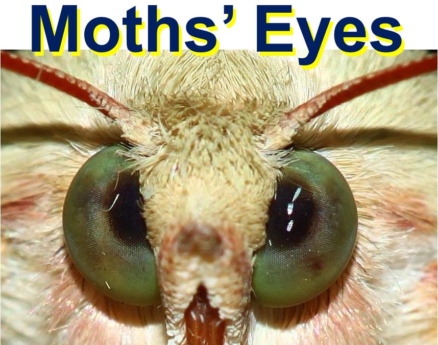 Moths can literally see in the dark. They have microscopic patterning that allows them to see in the dimmest environments. The Surrey scientists said they got inspiration from nature – specifically how moths see – when they were researching the potential applications of graphene. (Image: naturesbeststudents.org)
Prof. Silva and colleagues now plan to incorporate the material they created into several existing and emerging technologies.
Prof. Silva said:
“We are very excited about the potential to exploit this material in existing optical devices for performance enhancement, whilst looking towards new applications.”
“Through Surrey’s EPSRC funded Graphene Centre, we are looking for industry partners to exploit this technology and are keen to hear from innovative companies who we can explore the future applications of this technology with us.”
The technology was developed by the Surrey University team, in cooperation with BAE Systems for infrared imaging in opto-MEMs devices.
Citation: “Ultra-broadband light trapping using nanotextured decoupled graphene multilayers,” José V. Anguita, Muhammad Ahmad, Sajad Haq, Jeremy Allam and S. Ravi P. Silva. Science Advances Vol. 2, no. 2, e1501238. 26 February, 2016. DOI: 10.1126/sciadv.1501238.
Video – What is Graphene?
This short animation, produced by the University of Manchester in England, takes a look at how graphene was isolated and answers the widely asked question – What is graphene?
Comments are closed.