A team of scientists has demonstrated a novel mechanism that may help develop smaller and faster electronic devices. Electronic devices and their prevalence have transformed how we live in the twenty-first century. They have transformed how we work, rest, and also how we play. At the heart of electronic devices is the movement of electrons across materials.
OIST scientists demonstrate new ways to move and manipulate electrons. OIST stands for Okinawa Institute of Science and Technology Graduate University. There is currently a race among researchers globally to make better and faster functioning devices.
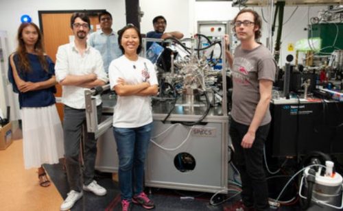
Keshav Dani and colleagues have written about their study and achievements in the journal Science Advances (citation below). Dani is an Associate Professor at OIST’s Femtosecond Spectroscopy Unit. Co-authors E Laine Wong, Andrew J. Winchester, Vivek Pareek, Julien Madéo, and Michael K. L. Man are also from OIST’s Femtosecond Spectroscopy Unit.
New mechanism for creating electronic devices
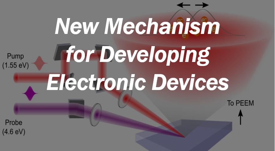
The researchers have demonstrated a new mechanism for developing electronic devices. This mechanism could potentially allow the control of electrons on the nanometer spatial scale and femtosecond temporal scales using light. A nanometer is 10-9 (one billion) of a meter, while a femtosecond is a 10-15 (one quadrillionth) of a second.
If we apply a voltage across a semiconducting material, it subsequently generates an electric field. The field directs the electron flow through the material. Dr. E. Laine Wong and colleagues have used the surface photovoltage effect to induce electric fields on the material. Dr. Wong is a recent PhD graduate at OIST.
The surface photovoltage effect is an effect in which a material’s surface potential can be varied by altering the light intensity.
Dr. Wong said:
“By making use of the nonuniform intensity profile of a laser beam, we manipulate the local surface potentials to create a spatially varying electric field within the photoexcitation spot. This allows us to control electron flow within the optical spot.”
Electron microscopy and femtosecond spectroscopy techniques
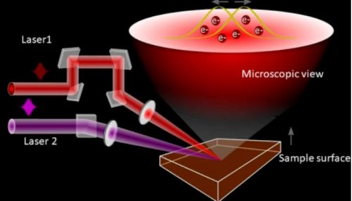
The scientists made a movie of the flow of electrons on femtosecond timescales. They used a combination of electron microscopy and femtosecond spectroscopy techniques.
In femtosecond spectroscopy, for example, researchers use an ultrafast laser beam to excite the electrons in the sample. We call that laser beam the ‘pump.’
A second ultrafast laser beam is then shone upon the sample to monitor the evolution of the excited electrons. We call this second laser beam the ‘probe.’ Hence, we refer to this technique as pump-probe spectroscopy.
The technique has allowed the researchers to study the excited electron’s dynamics at an extremely short time-scale.
The combination of an electron microscope then provides the researchers with the spatial resolution they need. Specifically, the spatial resolution they need to image the movement of the excited electrons directly. They can do this even within the tiny area of the laser beam spot.
Dr. Wong said:
“The combination of these two methods with both high spatial and temporal resolutions has allowed us to record a movie of the electrons being directed to flow in opposite directions.”
The authors say their study findings are also promising for controlling electron movement beyond the resolution of light. It is possible, for example, by utilizing the laser beams spatial intensity variations within the focal spot.
Creating electronic devices
Therefore, potentially, we could use the mechanism to operate nanoscale electronic circuits.
Prof. Dani and colleagues are currently working towards building electronic devices based on this newfound mechanism. Specifically, functional nanoscale, ultra-fast, electronic devices.
Citation
“Pulling apart photoexcited electrons by photoinducing an in-plane surface electric field,” E Laine Wong, Andrew J. Winchester, Vivek Pareek, Julien Madéo, Michael K. L. Man, and Keshav M. Dani. Science Advances 07 Sep 2018: Vol. 4, no. 9, eaat9722. DOI: 10.1126/sciadv.aat9722.
Video – Flow of electrons
The flow of electrons on femtosecond timescales.