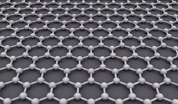
Graphene is on the way to superconductivity, says a team of scientists. Carbon atoms have several possibilities to form bonds. Therefore, pure carbon exists in many different forms. It can exist as, for example, diamond, football molecules, and nanotubes. It can also exist as a honeycomb-net with hexagonal meshes; in other words, graphene.
Graphene is the strongest and lightest substance we know of. It is approximately two hundred times stronger than the strongest steel. It also conducts electricity and heat efficiently
Graphene is not a superconductor. This, however, may be changed, says a team of scientists.
D. Marchenko, D. V. Evtushinsky, E. Golias, A. Varykhalov, Th. Seyller, and O. Rader wrote about their work in the journal Science Advances (citation below).
What is superconductivity?
Superconductivity is the ability of some materials to conduct electric current with practically zero resistance.
According to an article on the website of the University of Alaska Fairbanks:
“A superconductor is a material that can conduct electricity or transport electrons from one atom to another with no resistance.”

Superconductivity with graphene is complicated
In April this year, an MIT team showed that it is possible to generate a form of superconductivity in a system of two graphene layers. To achieve this required very specific conditions.
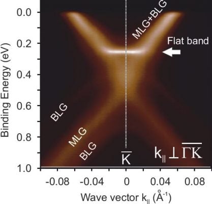
The scientists had to twist the two hexagonal nets against each other by exactly 1.1°. A flat band, under this condition, forms in the electronic structure.
Preparing samples from two layers of graphene from such a precise twist is extremely complex. It is also not suitable for mass production.
Despite all the complications and apparent drawbacks, the study has attracted a great deal of attention from other scientists.
Forming flat bands the simple way
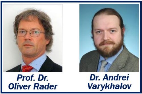
There is, however, one much simpler way of forming a flat band. A team at the HZB, led by Dr. Andrei Varykhalov and Prof. Oliver Rader, showed us how. HZB stands for Helmholtz Zentrum Berlin für Materialien und Energie (Berlin Helmholtz Center for Materials and Energy). HZB is part of the Helmholtz Association of German Research Centers.
Prof. Thomas Seyller, from Chemnitz University of Technology in Germany, provided the samples. Scientists used a process for producing them that is suitable for large-scale production. It is also suitable for larger area production.
The scientists heated a silicon carbide crystal until the silicon atoms evaporated from the surface. This left a single layer of graphene on the surface, and then a second layer also of graphene.
The two graphene layers lay precisely on top of each other and were not twisted against each other.
Angle-resolved photoemission spectroscopy (ARPES)
The Berliner Elektronenspeicherring-Gesellschaft für Synchrotronstrahlung m. b. H. (Berlin Electron Storage Ring Society for Synchrotron Radiation), abbreviated BESSY, is a research center that belongs to HZB. BESSY II, a storage ring, is the first third-generation synchrotron radiation source in Germany.
At BESSY II, scientists can scan the band structure of the sample. Regarding this band structure, HZB explained the following in a press release:
“This band structure provides information on how the charge carriers are distributed among the quantum-mechanically permitted states and which charge carriers are available for transport at all.”
“The angle-resolved photoemission spectroscopy (ARPES) at BESSY II enables such measurements with extremely high resolution.”
Using an exact analysis of the band structure, the researchers identified an area that scientists had previously overlooked.
Dr. Varykhalov explained:
“The double layer of graphene has been studied before because it is a semiconductor with a band gap. But on the ARPES instrument at BESSY II, the resolution is high enough to recognize the flat area next to this band gap.”
“It is an overseen property of a well-studied system”, first author Dr. Dmitry Marchenko points out: “It was previously unknown that there is a flat area in the band structure in such a simple well-known system.”

Superconductivity still requires a little help
This flat area is a prerequisite for superconductivity. However, only if it is located precisely at the Fermi energy. The Fermi energy is the highest occupied energy level of a material at absolute zero temperature (−273.15°C).
The two-layer graphene’s energy level is only 200 milli-electron volts below the Fermi energy. It is possible, however, to raise the flat area’s energy level to the Fermi energy. We can do this either by doping with foreign atoms or applying a gate voltage (an external voltage).
The researchers have found that the interactions between the two layers of graphene and between graphene and the silicon carbide lattice were jointly responsible for the flat band area formation.
Prof. Rader said:
“We can predict this behavior with very few parameters and could use this mechanism to control the band structure.”
Citation
“Extremely flat band in bilayer graphene,” D. Marchenko, D. V. Evtushinsky, E. Golias, A. Varykhalov, Th. Seyller, and O. Rader. Science Advances, 09 Nov 2018: Vol. 4, no. 11, eaau0059. DOI: 10.1126/sciadv.aau0059.

