
By manipulating the wrinkles which can form in graphene, researchers at the Surface and Interface Science Laboratory, RIKEN, Japan, believe the two-dimensional structure could be used as a semiconductor.
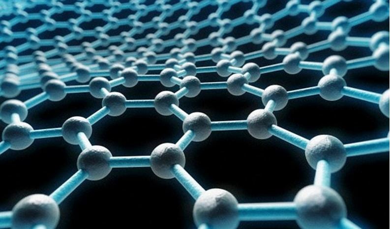
Graphene is a thin layer of pure carbon – a single, tightly-packed layer of carbon atoms that are bonded together in a hexagonal honeycomb lattice. This allotrope of carbon can form wrinkles which make the structure more complicated.
The graphene may also interact with the substrate (underlying substance or layer) it is laid upon, adding further complexity.
The RIKEN scientists explained in Nature Communications (citation below) that they have now discovered that wrinkles that form in graphene can restrict the electrons in one dimension, forming a junction-like structure that shifts from zero-gap conductor to semiconductor back to zero-gap conductor.
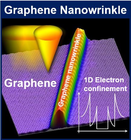 Schematic showing a graphene nanowrinkle. (Image: www.riken.jp)
They have manipulated the formation of wrinkles using the tip of a scanning tunneling microscope, thus opening a way to the construction of graphene semiconductors not by chemical means (with the addition of other elements), but through a form of ‘graphene engineering’ (manipulating the carbon structure itself).
The scientists made their discovery while experimenting with creating graphene films using chemical vapor deposition – the most reliable method we know of. They were working to form graphene on a nickel substrate, which depends heavily on the temperature and cooling speed.
First author, Hyunseob Lim, said:
“We were attempting to grow graphene on a single crystalline nickel substrate, but in many cases we ended up creating a compound of nickel and carbon, Ni2C, rather than graphene.”
“In order to resolve the problem, we tried quickly cooling the sample after the dosing with acetylene, and during that process we accidentally found small nanowrinkles, just five nanometers wide, in the sample.”
Nanowrinkles may act as semiconductors
With scanning tunneling microscopy they were able to image these minute wrinkles, and discovered that there were band gap openings within them, suggesting that the wrinkles might act as semiconductors.
Normally, electron holes and electrons flow freely through a conductor with no band gap. However, when it is a semiconductor there are band gaps between the permitted electron states, and the electrons are only able to pass through these gaps under certain conditions.
 Scanning tunneling microscope images of the graphene with the nanowrinkles. (Image: www.riken.jp)
This suggests that graphene could become a semiconductor, depending on the wrinkles.
At first, the researchers considered two possibilities for the emergence of this band gap. 1. The mechanical strain might cause a magnetic phenomenon. This was ruled out. 2. It was more likely caused by the confinement of electrons in a single dimension due to ‘quantum confinement’.
Team leader, Yousoo Kim, head of the Surface and Interface Science Laboratory, said:
“Up until now, efforts to manipulate the electronic properties of graphene have principally been done through chemical means, but the downside of this is that it can lead to degraded electronic properties due to chemical defects.”
“Here we have shown that the electronic properties can be manipulated merely by changing the shape of the carbon structure. It will be exciting to see if this could lead to ways to find new uses for graphene.”
Earlier this year, scientists at the Department of Energy’s Oak Ridge National Laboratory showed how it is possible to make large-scale graphene.
Citation: “Structurally driven one-dimensional electron confinement in sub-5-nm graphene nanowrinkles,” Hyunseob Lim, Jaehoon Jung, Rodney S. Ruoff & Yousoo Kim. Nature Communications. Published 23 October 2015. DOI: 10.1038/ncomms9601.
